


Introduction
The global electronics industry, which encompasses computers, business equipment, consumer, military and automotive electronics, has experienced remarkable growth in the past two decades and is now in excess of $1.5T a year. The RF/microwave industry, including test equipment, radar and wireless telecommunications is estimated to be over $100B a year. Although the packaging market segment of the RF/microwave industry, defined as IC packages, printed circuit boards (PCB), solder joining, wire bonding, cabling and connectors, represents less than 1% of the overall global electronics packaging industry, it is conservatively estimated to be a market segment of over $1.2B a year.
By now it will be appreciated that the concept of guided electromagnetic wave propagation, demonstrated by the reclusive genius Oliver Heaviside over 100 years ago, has evolved into a massive multi-national business enterprise which at the beginning of the 21st century, provides the basis for a new world economy. Mass production of electronic equipment can be traced back to the Second World War with the hand soldering of discrete components and rather primitive circuit boards for radar applications. In the 1950s, wave solder technology for through-hole components enabled high-volume production of printed circuit boards. This technology has proven to be the backbone of the electronics industry for almost fifty years.
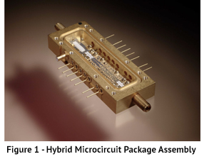 However, in the 1980s the advent of machine vision and pattern recognition fostered use of automated surface mount technology (SMT), resulting in dramatic densification of electronic assemblies. Initially, surface mount components were peripherally leaded packages with a limited maximum lead count. But in the early 1990s, the pressure to increase interconnect densities led to development of ball grid array (BGA) packages. Although BGA technology is less expensive, thinner, lighter and more easily integrated into circuit board architectures than conventional hybrid microwave integrated circuit packages (see Figure 1), issues with shielding, isolation and interconnection serve as drawbacks for RF/microwave subsystem applications. In the mid-1990s the evolution of flip-chip technology (FCT) overcame some of the limitations of BGA for higher frequency applications and improved on interconnect density. The advent of FCT was driven by digital applications such as high-end microprocessors, disk drive ICs, watches, and automotive ignition units. Consequently, flip-chip infrastructure developed rapidly. More recently, flip-chip device technology has been employed for applications in the mm-wave region such as automotive radar. As the requirements for SMT, BGA and FCT based applications have moved to higher frequencies, the need for high performance coaxial connectors that interface directly to planar substrates has increased dramatically.
A Coaxial Connector for Planar Substrates
The primary method for routing high frequency signals between circuit modules in instruments and test systems is via semi-rigid coaxial cables. While coaxial cables provide a radially symmetric transmission structure for the signals, the transmission structures within the circuit modules are inherently planar. Generally, these structures incorporate microstrip transmission lines on a planar substrate. Due to requirements for signal isolation and low inductance, the electrical transition between the radially symmetric coaxial cable and planar microstrip environment is not only critical to the electrical performance of the system, but also technically challenging from both a design and manufacturing standpoint. This is particularly true for signals propagated in the microwave or millimeter wave frequency range where discontinuities at the transition interface cause impedance mismatches that can significantly degrade the electrical signal. The traditional approach for minimizing discontinuities and impedance mismatches between coaxial and planar transmission structures for high frequency applications is to orient the center conductor of a coaxial connector assembly parallel to the plane of the circuit module’s microstrip transmission line. This type of interface entails attaching the device substrate to the floor of a metal package body (Figure 1) and then threading the connector assembly into a tapped hole in the wall of the package body. The position of the tapped hole aligns the center conductor with the planar transmission structure. Although this configuration results in favorable impedance matching at the interface, the fact that it relies on a metal package body increases the size and manufacturing cost of the circuit module. This article presents a high performance glass-to-metal seal based coaxial connector which can be affixed directly to the planar substrate of a circuit module or printed circuit board, allowing the circuit module to be smaller and less expensive than conventional hybrid microcircuit package assemblies.
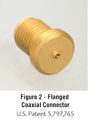 In practice, the connector is attached directly to a planar substrate using solder or conductive epoxy. The substrate material can be ceramic, polymeric or a metal alloy, with suitable contact pads to foster the attachment process and assure electrical continuity. The connector is designed to mount perpendicular to the substrate and provide a transition between the circuit module and a semi-rigid cable. A cylindrical conductive bore, with a radially symmetric coaxial structure, is fabricated in the substrate to provide an impedance match between the coaxial and planar transmission structures. The mating surface of the connector is flanged to afford maximum contact area (see Figure 2). This insures electrical contact and enhances the mechanical stability of the assembly. A center pin protrudes through a hole in the flange, which has a nipple formed around it. The nipple serves to align the pin in the conductive bore of the substrate during the attachment process so that a symmetric coaxial transition is maintained. The circuit is completed with a suitable bond between the planar transmission line on the opposite side of the substrate and the end of the connector center pin extending through the substrate bore.
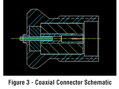 Figure 3 shows an engineering drawing of the coaxial connector under consideration. The connector assembly is comprised of five lower level components: an outer conductor or housing, a glass bead, a center pin, a dielectric support bead, and a center conductor. Although surface mountable connectors do not generally require hermeticity, this connector features an integral glass-to-metal seal to enhance mechanical stability and precisely locate the center pin in the housing through hole. The position of the center pin in the RF through hole is critical to the propagation of electrical signals as they exit the coaxial structure. The other end of the connector provides a transition to the external coaxial environment, in this case an SMA coplanar pin-and-socket style interface. To accomplish that, the connector housing is threaded on the outside to receive a standard semi-rigid cable coupling. The center conductor is a slotted female contact with the end of the center conductor coincident with the mating plane of the connector housing. The center conductor is supported by a polytetrafluoroethylene (PTFE) dielectric bead, which is held in place via knurls on the outer diameter of the center conductor as well as notches on the inner diameter of the housing, just below the mating reference plane. The reliability of the mating interface geometry with respect to repeated connections is enhanced by the configuration described. This coaxial connector is designed and electrically compensated to function at frequencies in the 10 GHz range with exceptional electrical performance.
Controlled Expansion Alloys
A key design aspect of SMT connectors is the material selection for the housing (outer conductor), which in turn drives the material selection for the center pin (center conductor) and to a lesser degree the glass bead. A number of controlled expansion alloys can be employed in the fabrication of the connector housing, but the material selection depends on the substrate material the connector will be attached to (PCB or ceramic) and the particular method of attachment (epoxy or solder). For example, an SMT connector designed for solder attachment to a metallized planar ceramic substrate, say Alumina (Al2O3) with a coefficient of thermal expansion (CTE) of about 8.2 ppm/°C, the selected housing material would be Alloy 42® with a CTE of 7 ppm/°C. In this case, the center pin could be either Alloy 42® or Kovar® with a CTE of 5.3 ppm/°C. Other commonly used ceramic substrate materials include Aluminum Nitride (AlN) with a CTE of 4.5 ppm/°C, Silicon Carbide (SiC) with a CTE of 4 ppm/°C and Macor®, a machinable ceramic with a CTE of 9 ppm/°C. For the AlN and SiC ceramic substrates the connector housing and center pin would be fabricated using Kovar®. For a Macor® substrate the housing material is Alloy 46® or Alloy 48®. When solder is preferred (generally for strength and electrical conductivity), the rule of thumb for the difference in CTEs is less than 5 ppm/°C. Because conductive epoxy is more compliant, close matching of the connector housing and substrate CTEs is not as critical.
However, when mounting SMT connectors on laminated PCB material, the CTE relationships are very different. Most FR-4 laminates have a CTE in the 14 ppm/°C range, which is considerably higher than ceramic substrates. But modern PCB laminate stacks now contain metal cores made from copper-invar-copper (CIC) or copper-molybdenum-copper (CMC) stacks, with CTEs of 8 ppm/°C and 6 ppm/°C, respectively. These metal cores serve to anchor the expansion of the FR-4 outer layers and provide overall CTEs of 12 ppm/°C for the CIC and 9 ppm/°C for the CMC PCB laminate stacks. So, when attaching SMT connectors to hybrid PCB laminate structures the preferred controlled expansion alloy for the connector housing is Alloy 48®, with a CTE of 9 ppm/°C, for CIC anchored substrates and Alloy 46®, with a CTE of 7.9 ppm/°C when the substrate is CMC anchored. The center pin material is Alloy 42® and Kovar®, respectively. The CTE values for the germane materials are summarized in Table 1.
Table 1 – Coefficient of Thermal Expansion for Packaging Materials
| Material | SiC | AIN | Al2O3 | Macor® | FR-4 PCB | CIC PCB | CMC PCB | Kovar® | Alloy 42 |
| CTE (ppm/°C) | 4 | 4.5 | 8.2 | 9 | 14 | 12 | 9 | 5.3 | 7 |
Case Study
 The commercial state of the art for high-speed digital communication systems has now pushed beyond the previous 2.5 Gb/s to above 10 Gb/s. The advent of dense wavelength division multiplexing (DWDM), with up to 128 wavelength channels co-propagating on a single optical fiber, has generated an aggregate communication bandwidth which exceeds the terabit per second level. With these astonishing technological advances in bit rate and wavelength density, it is not surprising that the most important parameter for a digital communications system is the rate at which errors occur in the data bit stream. This figure of merit is a statistical parameter called the bit-error ratio (BER). The now obsolete Keysight (formerly Agilent) 86130A instrument was a 3.6 Gb/s general purpose BER tester designed for high-speed digital communication applications. This advanced BER tester was employed in design, manufacturing and quality assurance test environments to characterize the performance of photonic systems, components and fibers.
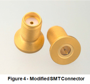
 The 86130A BER tester was one of the first instruments to make use of chip-on-board technology. As such, a number of surface mount coaxial connectors were employed for both signal input and output functions to and from the modules. Figure 4 is a photograph showing both ends of the connector, which is a modified version of the coaxial connector described previously. The flange on this connector does not utilize a through hole, but rather the glass-to-metal seal interface is coincident with the flange surface. The coaxial mating interface is identical to the connector previously described. The photograph in Figure 5 shows three surface mount coaxial connectors in close proximity on the pattern generator module board. This connector design is very robust, mechanically and electrically, and was a key enabling factor for the high performance and reasonable manufacturing cost of the pattern generator and error detector modules for the 86130A.
Conclusion
It is clear that advances in surface mount, ball grid array and flip-chip technologies have created a need for high performance coaxial connectors that can be attached directly to planar substrates. A glass-to-metal seal based coaxial connector has been developed to satisfy the requirement for a surface mountable connector that provides a low inductance transition between radially symmetric and planar signal transmission structures at microwave and mm-wave frequencies. A key enabling factor in the design of these connectors is the selective use of controlled expansion alloys to customize the attachment method for various substrate materials. This connector was effectively utilized in a next generation bit-error ratio test instrument for the digital communications market.